- 您现在的位置:买卖IC网 > Sheet目录329 > IDT70V7319S166BCI (IDT, Integrated Device Technology Inc)IC SRAM 4MBIT 166MHZ 256BGA
�� �
�
�IDT70V7319S�
�High-Speed� 256K� x� 18� Synchronous� Bank-Switchable� Dual-Port� Static� RAM�
�Industrial� and� Commercial� Temperature� Ranges�
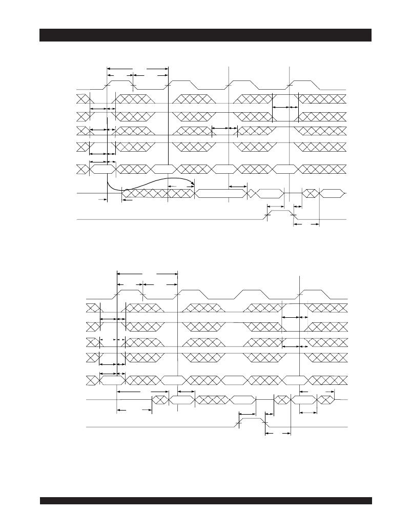
�Timing� Waveform� of� Read� Cycle� for� Pipelined� Operation�
�(� ADS� Operation)� (PL/� FT� 'X'� =� V� IH� )� (2)�
�t� CYC2�
�CLK�
�CE� 0�
�t� CH2�
�t� CL2�
�t� SC�
�t� HC�
�t� SC�
�t� HC�
�(3)�
�CE� 1�
�UB� /� LB�
�R/� W�
�t� SB�
�t� SW�
�t� SA�
�t� HB�
�t� HW�
�t� HA�
�t� SB�
�(5)�
�t� HB�
�ADDRESS�
�(4)�
�An�
�An� +� 1�
�An� +� 2�
�An� +� 3�
�(1� Latency)�
�t� CD2�
�t� DC�
�DATA� OUT�
�t� CKLZ�
�(1)�
�Qn�
�Qn� +� 1�
�t� OHZ�
�t� OLZ�
�Qn� +� 2�
�(5)�
�OE�
�(1)�
�t� OE�
�5629� drw� 06�
�Timing� Waveform� of� Read� Cycle� for� Flow-through� Output�
�(PL/� FT� "X"� =� V� IL� )� (2,6)�
�t� CYC1�
�CLK�
�CE� 0�
�t� CH1�
�t� CL1�
�t� SC�
�t� HC�
�t� SC�
�t� HC�
�CE� 1�
�t� SB�
�t� HB�
�(3)�
�BE� n�
�R/� W�
�t� SW� t� HW�
�t� SA�
�t� HA�
�t� SB�
�(5)�
�t� HB�
�ADDRESS�
�(4)�
�An�
�t� CD1�
�An� +� 1�
�t� DC�
�An� +� 2�
�An� +� 3�
�t� CKHZ�
�DATA� OUT�
�Qn�
�Qn� +� 1�
�Qn� +� 2� (5)�
�NOTES:�
�OE�
�(1)�
�t� CKLZ�
�t� OHZ�
�t� OLZ�
�t� OE�
�t� DC�
�5629� drw� 07�
�1.� OE� is� asynchronously� controlled;� all� other� inputs� are� synchronous� to� the� rising� clock� edge.�
�2.� ADS� =� V� IL� ,� CNTEN� and� REPEAT� =� V� IH� .�
�3.� The� output� is� disabled� (High-Impedance� state)� by� CE� 0� =� V� IH� ,� CE� 1� =� V� IL� ,� UB� /� LB� =� V� IH� following� the� next� rising� edge� of� the� clock.� Refer� to�
�Truth� Table� 1.�
�4.� Addresses� do� not� have� to� be� accessed� sequentially� since� ADS� =� V� IL� constantly� loads� the� address� on� the� rising� edge� of� the� CLK;� numbers�
�are� for� reference� use� only.�
�5.� If� UB� /� LB� was� HIGH,� then� the� appropriate� Byte� of� DATA� OUT� for� Qn� +� 2� would� be� disabled� (High-Impedance� state).�
�6.� "x"� denotes� Left� or� Right� port.� The� diagram� is� with� respect� to� that� port.�
�11�
�6.42�
�发布紧急采购,3分钟左右您将得到回复。
相关PDF资料
IDT70V7339S166BCI
IC SRAM 9MBIT 166MHZ 256BGA
IDT70V7519S166DRI
IC SRAM 9MBIT 166MHZ 208QFP
IDT70V7599S133DRI
IC SRAM 4MBIT 133MHZ 208QFP
IDT70V9089L6PF
IC SRAM 512KBIT 6NS 100TQFP
IDT70V9169L7BFI
IC SRAM 144KBIT 7NS 100FBGA
IDT70V9189L9PFI
IC SRAM 576KBIT 9NS 100TQFP
IDT70V9199L9PFI
IC SRAM 1.125MBIT 9NS 100TQFP
IDT70V9279L7PRFI
IC SRAM 512KBIT 7NS 128TQFP
相关代理商/技术参数
IDT70V7319S166BCI8
功能描述:IC SRAM 4MBIT 166MHZ 256BGA RoHS:否 类别:集成电路 (IC) >> 存储器 系列:- 标准包装:3,000 系列:- 格式 - 存储器:EEPROMs - 串行 存储器类型:EEPROM 存储容量:8K (1K x 8) 速度:400kHz 接口:I²C,2 线串口 电源电压:1.7 V ~ 5.5 V 工作温度:-40°C ~ 85°C 封装/外壳:8-SOIC(0.154",3.90mm 宽) 供应商设备封装:8-SOIC 包装:带卷 (TR)
IDT70V7319S166BF
功能描述:IC SRAM 4MBIT 166MHZ 208FBGA RoHS:否 类别:集成电路 (IC) >> 存储器 系列:- 标准包装:3,000 系列:- 格式 - 存储器:EEPROMs - 串行 存储器类型:EEPROM 存储容量:8K (1K x 8) 速度:400kHz 接口:I²C,2 线串口 电源电压:1.7 V ~ 5.5 V 工作温度:-40°C ~ 85°C 封装/外壳:8-SOIC(0.154",3.90mm 宽) 供应商设备封装:8-SOIC 包装:带卷 (TR)
IDT70V7319S166BF8
功能描述:IC SRAM 4MBIT 166MHZ 208FBGA RoHS:否 类别:集成电路 (IC) >> 存储器 系列:- 标准包装:3,000 系列:- 格式 - 存储器:EEPROMs - 串行 存储器类型:EEPROM 存储容量:8K (1K x 8) 速度:400kHz 接口:I²C,2 线串口 电源电压:1.7 V ~ 5.5 V 工作温度:-40°C ~ 85°C 封装/外壳:8-SOIC(0.154",3.90mm 宽) 供应商设备封装:8-SOIC 包装:带卷 (TR)
IDT70V7319S166DD
功能描述:IC SRAM 4MBIT 166MHZ 144TQFP RoHS:否 类别:集成电路 (IC) >> 存储器 系列:- 产品变化通告:Product Discontinuation 26/Apr/2010 标准包装:136 系列:- 格式 - 存储器:RAM 存储器类型:SRAM - 同步,DDR II 存储容量:18M(1M x 18) 速度:200MHz 接口:并联 电源电压:1.7 V ~ 1.9 V 工作温度:0°C ~ 70°C 封装/外壳:165-TBGA 供应商设备封装:165-CABGA(13x15) 包装:托盘 其它名称:71P71804S200BQ
IDT70V7319S166DDI
功能描述:IC SRAM 4MBIT 166MHZ 144TQFP RoHS:否 类别:集成电路 (IC) >> 存储器 系列:- 产品变化通告:Product Discontinuation 26/Apr/2010 标准包装:136 系列:- 格式 - 存储器:RAM 存储器类型:SRAM - 同步,DDR II 存储容量:18M(1M x 18) 速度:200MHz 接口:并联 电源电压:1.7 V ~ 1.9 V 工作温度:0°C ~ 70°C 封装/外壳:165-TBGA 供应商设备封装:165-CABGA(13x15) 包装:托盘 其它名称:71P71804S200BQ
IDT70V7319S200BC
功能描述:IC SRAM 4MBIT 200MHZ 256BGA RoHS:否 类别:集成电路 (IC) >> 存储器 系列:- 标准包装:3,000 系列:- 格式 - 存储器:EEPROMs - 串行 存储器类型:EEPROM 存储容量:8K (1K x 8) 速度:400kHz 接口:I²C,2 线串口 电源电压:1.7 V ~ 5.5 V 工作温度:-40°C ~ 85°C 封装/外壳:8-SOIC(0.154",3.90mm 宽) 供应商设备封装:8-SOIC 包装:带卷 (TR)
IDT70V7319S200BC8
功能描述:IC SRAM 4MBIT 200MHZ 256BGA RoHS:否 类别:集成电路 (IC) >> 存储器 系列:- 标准包装:3,000 系列:- 格式 - 存储器:EEPROMs - 串行 存储器类型:EEPROM 存储容量:8K (1K x 8) 速度:400kHz 接口:I²C,2 线串口 电源电压:1.7 V ~ 5.5 V 工作温度:-40°C ~ 85°C 封装/外壳:8-SOIC(0.154",3.90mm 宽) 供应商设备封装:8-SOIC 包装:带卷 (TR)
IDT70V7339S133BC
功能描述:IC SRAM 9MBIT 133MHZ 256BGA RoHS:否 类别:集成电路 (IC) >> 存储器 系列:- 标准包装:3,000 系列:- 格式 - 存储器:EEPROMs - 串行 存储器类型:EEPROM 存储容量:8K (1K x 8) 速度:400kHz 接口:I²C,2 线串口 电源电压:1.7 V ~ 5.5 V 工作温度:-40°C ~ 85°C 封装/外壳:8-SOIC(0.154",3.90mm 宽) 供应商设备封装:8-SOIC 包装:带卷 (TR)